©2022 Thai Microelectronics Center. All Right Reserved..

services
Characterization
We offer an extensive variety of analytical approaches for different materials characterization and testing services.
TMEC provide a responsive, confidential and professional contract surface analysis service to both the industrial and academic sectors.
We offer an extensive variety of analytical approaches for different materials characterization and testing services. With over 20 years of experience in materials characterization, we provide the best solution or combination techniques to solve your problems.
No matter what your characterization and analysis require, TMEC can provide the most applicable techniques to reveals the answers you need. TMEC has a service networking via more than 20 certified national laboratories and national research centers. Fast-track service to support our valuable customers. All the analytical techniques are for the analysis of surface topology, surface morphology, film thickness, interface qualities and interface sharpness, compositions and depth profiles of solid samples.
TMEC’s materials characterization services can be applied to various fields including:

Research & development:
For basic research and the testing of new concepts and materials and theirs surface properties

Production:
To qualify incoming materials; monitoring; quality control

Failure analysis:
To investigate problems for contamination/defect analysis and to identify contaminant sources
Material characterization
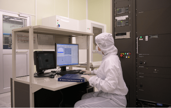
Auger electron spectroscopy (or Auger, AES)
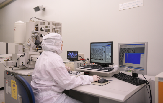
Field-emission Scanning Electron Microscopy (FE-SEM) is an imaging technique where a focused electron beam is raster scanning across the sample surface to generate several different types of emission. The backscattered secondary electron that pass through a backscattered electron detector can provide a high-resolution and high-magnification micrographs. Our high resolution FE-SEM is integrated with energy dispersive x-ray spectroscopy (EDX) and X-ray fluorescence (XRF) to provide a surface characteristic of the element on the sample surface.
Currently, the AES lab is out-of-service. Please contact us and we will notify you by email when it is ready.
Material characterization
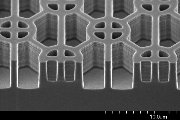
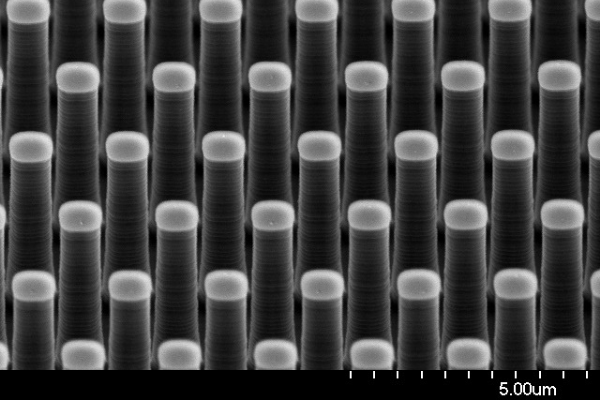
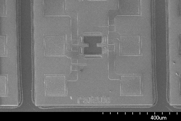
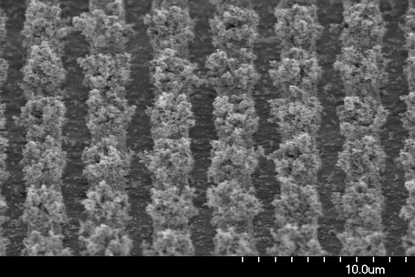
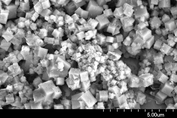
Field-emission Scanning Electron Microscopy (FE-SEM)
Field-emission Scanning Electron Microscopy (FE-SEM) is an imaging technique where a focused electron beam is raster scanning across the sample surface to generate several different types of emission. The backscattered secondary electron that pass through a backscattered electron detector can provide a high-resolution and high-magnification micrographs. Our high resolution FE-SEM is integrated with energy dispersive x-ray spectroscopy (EDX) and X-ray fluorescence (XRF) to provide a surface characteristic of the element on the sample surface.
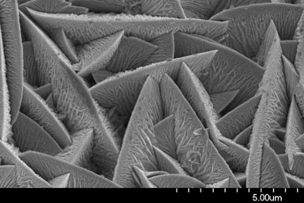
FE-SEM image by TMEC
.
.
.
.
.
.
Material characterization
Energy Dispersive X-ray Spectroscopy (EDS or EDX)
Energy Dispersive X-ray Spectroscopy (EDS or EDX) is a technique for analyzing the elements from boron to uranium of solid materials in sub- micrometer space. The distribution of the elements can be analyzed and shown in a map (Mapping). The element can be detected as low as 0.1 percent by weight (wt.%).
Material characterization
Technical comparison
| Technique | FE-SEM | EDX | AES |
|---|---|---|---|
| Probe | Electrons | Electrons | Electrons |
| Detection | Secondary and backscattered electrons | X-rays | Auger Electrons |
| Collected Data | Pictures | Qualitative elemental analysis | Elemental Composition |
| Typical Analysis Area | 1.5 nm (500,000 X) | 100nm–1um | 10nm–10um |
| Typical Analysis Dept rang | 1-100 nm | um | 10 nm |
| Type of experiments | Metal Oxides Ceramics Polymers Nanomaterials Powder Glasses Bio-materials Semiconductors Rubber | Metals glass ceramics Polymers Film oxides | Metal Oxides Ceramics Polymers Nanomaterials Powder Glasses Bio-materials Semiconductors |
Electrical characterization
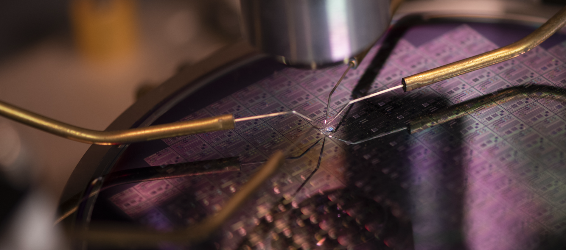
Electrical characterization is crucial for semiconductor and MEMS devices. TMEC can perform electrical characterization of devices in a test fixture or on wafers (up to 8 inches) using the semiconductor device parameter analyzer Agilent B1500A in manual and semiautomatic probe stations. The measuring instrument can analyze current-voltage characteristics (I-V), capacitance-voltage (C-V), calculate basic device properties, and automatically report the results. A heating chuck for up to 6-inch wafers is available, allowing the wafer to be heated up to 200 °C. A microscope with an integrated high-resolution camera provides the possibility to observe the wafer and device in real-time.
| Measurement system capabilities | |
|---|---|
| Agilent B1500A (now Keysight) | |
| One High-power SMU |
|
| Three High-resolution SMUs |
|
| Multi-frequency capacitance measurement unit |
|
| Precision LCR Meter HP4284A |
|
| Probe station (Cascade Microtech M150) |
|
| Probe station (Cascade Microtech Alessi REL-6100) |
|
Thai Microelectronics Center (TMEC)
51/4 Moo 1, Wangtakien District,
Amphur Muang, Chachoengsao,
Thailand 24000
Tel: +66 38 857 100-8,
+66 62 779 6111
Mobile: +66 92 687 1112
Fax: +66 38 857 175
E-mail: info-tmec@nectec.or.thA Subsidiary of:


Affiliates