©2022 Thai Microelectronics Center. All Right Reserved..
services
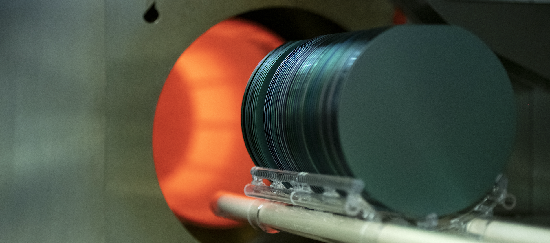
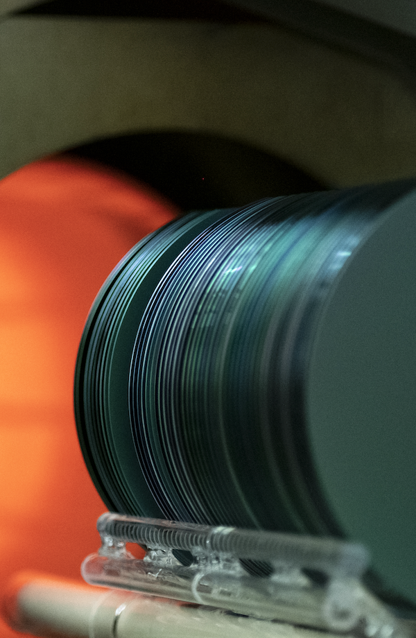
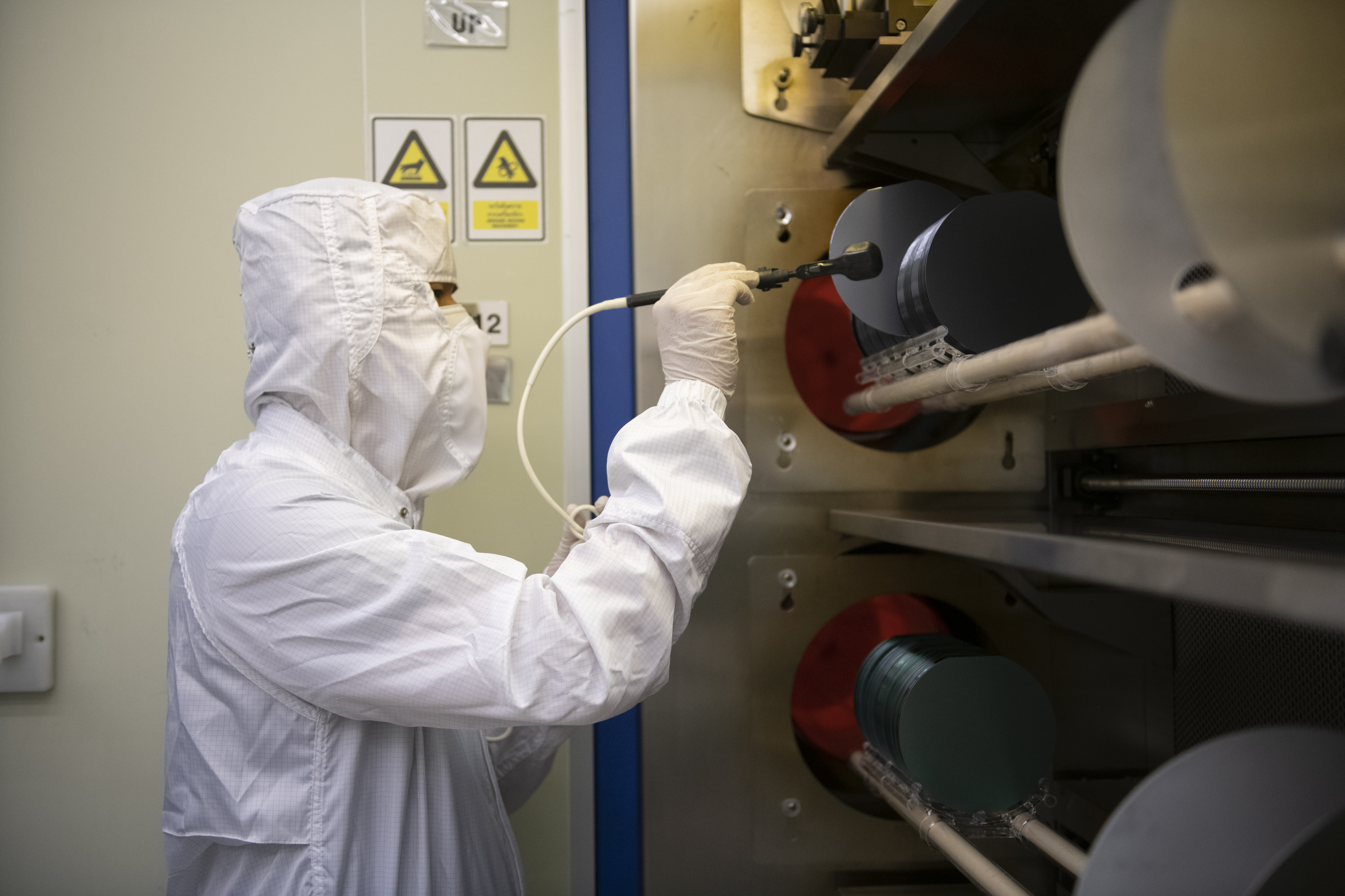
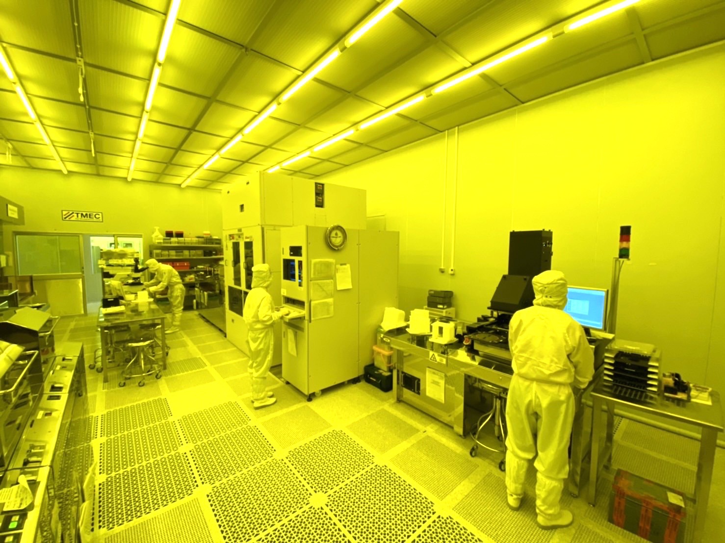
Micro/Nano
Fabrication
What We Offer:
- • 6-inch wafer fabrication
- • CMOS and CMOS-compatible process
- • Prototyping and small-scale production
- • Wafer processing: thin film, patterning, etching, etc.
Process Capabilities:
Thin film
- • Thermal oxidation (SiO2)
- • Sputtering (AlCuSi, Ti, TiN)
- • Low pressure chemical vapor deposition (TEOS oxide, Si3N4, Undoped polysilicon)
- • Plasma-enhanced chemical vapor deposition (SiO2, Si3N4)
- • Spin-on-glass film
Photolithography
- • I-line 365nm stepper
- • EVG 620 NT mask aligner
Etching
- • Reactive ion etching (Polysilicon, SiO2, Si3N4, AlCuSi, Ti, TiN)
- • Deep reactive ion etching (Si)
- • Wet etching (SiO2, Si, Al)
- • HF vapor etching (SiO2)

Ion Implantation
- • Phosphorus ions: P+ and P++
- • Boron ions: B+ and B++
- • Arsenic ions: As+

Thai Microelectronics Center (TMEC)
51/4 Moo 1, Wangtakien District,
Amphur Muang, Chachoengsao,
Thailand 24000
Tel: +66 38 857 100-8,
+66 62 779 6111
Mobile: +66 92 687 1112
Fax: +66 38 857 175
E-mail: info-tmec@nectec.or.thA Subsidiary of:


Affiliates